Introduction
A PCB failure in a controlled office environment is an inconvenience. In a downhole oil sensor, an aerospace guidance system, or a medical device, it's a different problem entirely—one measured in halted production lines, safety incidents, or mission failures.
The financial stakes are real. Siemens' 2024 True Cost of Downtime report found that unplanned downtime costs Fortune Global 500 industrial companies nearly $1.5 trillion annually—equivalent to 11% of revenues. Many of those failures trace back to components that simply weren't specified for the environment they ended up in.
Getting that specification right is the focus of this guide. It covers the full material reliability picture for engineers designing PCBs destined for demanding deployments:
- How harsh conditions cause specific failure modes
- Which substrate materials match which stressor profiles
- How conformal coatings and surface finishes extend field life
- What testing standards validate a board is ready before it ships
Key Takeaways
- Standard FR-4 fails in most harsh environments; always match substrate choice to your dominant stressor profile
- CTE mismatch, moisture absorption, and vibration fatigue are the three leading failure mechanisms
- High-Tg FR-4, polyimide, Rogers laminates, and metal-core substrates each address distinct failure modes
- Conformal coating type matters as much as thickness — Parylene consistently outperforms acrylic in severe environments
- IPC Class 3, thermal cycling, and humidity testing are non-negotiable for mission-critical qualification
What Qualifies as a "Harsh Environment" for PCBs?
Standard commercial-grade PCBs are designed for benign conditions: stable indoor temperatures, low humidity, minimal vibration. Six stressor categories push beyond those assumptions:
| Stressor | Industries Most Affected |
|---|---|
| Extreme temperature / thermal cycling | Automotive, industrial automation, oil & gas |
| Humidity and moisture | Marine, medical, outdoor infrastructure |
| Vibration and mechanical shock | Aerospace, defense, heavy equipment |
| EMI | Military, telecom, radar systems |
| Chemical and corrosive exposure | Oil & gas, marine, industrial processing |
| Altitude and pressure variation | Aerospace, military aviation |
Most engineers treat "harsh environment" as a single-stressor problem — that's where designs fail. A downhole oil sensor faces heat, pressure, vibration, and chemical exposure simultaneously. Optimizing only for thermal performance while ignoring chemical resistance produces a board that passes qualification testing and corrodes in the field.
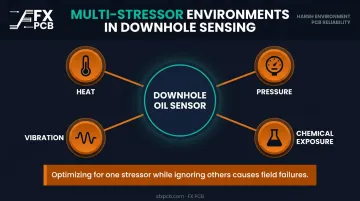
Map every stressor your application will face before touching the materials spec. The rest of the design process follows from that list.
How Harsh Conditions Cause PCB Material Failure
Thermal Stress and Delamination
The core mechanism is CTE (Coefficient of Thermal Expansion) mismatch. When a substrate expands and contracts at a different rate than copper traces or component pads during thermal cycling, it creates cumulative mechanical stress at the interface.
The damage accumulates incrementally: delamination of laminate layers, pad cratering, and micro-cracking in via barrels. These failures are often intermittent before becoming permanent, which makes them particularly difficult to catch during inspection.
The threshold behavior is important: standard FR-4 (Ventec VT-42) has a Tg of approximately 140°C with a Z-axis CTE of 50 ppm/°C pre-Tg that jumps to 250 ppm/°C post-Tg. Any board operating near or above Tg undergoes dramatic dimensional instability—warpage distorts fine-pitch component pads and controlled-impedance traces.
Moisture Absorption and Electrochemical Corrosion
Moisture absorbed into the substrate increases the dielectric constant, degrading signal integrity in high-frequency applications. More critically, trapped moisture combined with ionic contaminants (chlorides, bromides) creates electrochemical migration: the gradual growth of conductive dendrites between traces that eventually causes shorts.
NASA research identifies that halide residues accelerate dendritic growth, with rapid failure risk above 50 μg/in² contaminant levels. Surface-level effects include oxidation of exposed copper pads and increased contact resistance at connector interfaces.
Vibration and Mechanical Fatigue
Sustained vibration or repeated shock loads create fatigue crack initiation at predictable locations:
- Solder joint corners on large BGAs and heavy components
- Via barrel copper fractures
- Trace cracks at sharp corners
Thinner, lighter boards with minimal reinforcement are disproportionately vulnerable. Research shows that underfill beneath BGA packages can increase fatigue life exponentially. Applied at the layout stage, it's one of the lowest-cost interventions with the highest field-reliability return.
Chemical Degradation and EMI
Two additional failure mechanisms become significant in industrial and defense environments:
- Chemical attack: Aggressive solvents, fuels, and cleaning agents degrade conformal coatings and substrate surfaces over time, with failure rates accelerating at elevated temperatures
- EMI susceptibility: Without adequate grounding and shielding, signal noise causes data corruption or false triggering in sensitive circuits
Material selection directly determines resistance to both. Substrate chemistry governs chemical compatibility; copper plane design and shielding geometry govern EMI performance.
Selecting PCB Substrate Materials for Harsh Environments
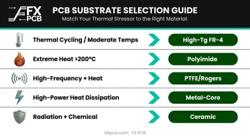
The selection principle: drive material choice from your dominant stressor profile, not from cost alone. Here's a practical decision framework:
| Primary Stressor | Recommended Substrate |
|---|---|
| Thermal cycling, moderate temps | High-Tg FR-4 (Tg ≥ 170°C) |
| Extreme heat (>200°C) | Polyimide |
| High-frequency signal stability + heat | PTFE / Rogers laminates |
| Heat dissipation from high-power components | Metal-core (aluminum or copper) |
| Radiation and chemical exposure | Ceramic (AlN, Al₂O₃) |
High-Tg FR-4: The Practical First Upgrade
Standard FR-4 has a Tg of 130–140°C—inadequate for applications exceeding 100°C operating temperature or wide thermal cycling ranges. High-Tg FR-4 (Tg ≥ 170°C) addresses this directly.
The Isola IS420, for example, specifies Tg at 170°C, moisture absorption at 0.15%, and Z-axis CTE of 45 ppm/°C pre-Tg—measurable improvements over standard grades. It's the cost-effective upgrade for industrial and automotive applications where chemical or radiation resistance isn't a simultaneous requirement.
SFX PCB fabricates high-Tg boards at Tg150, Tg170, and Tg180 grades, covering the range from moderate industrial to aerospace and medical applications.
Polyimide: For Extreme Thermal Demands
Polyimide substrates reach a Tg of 250°C (Ventec VT-901), with a Z-axis CTE of 50 ppm/°C pre-Tg and only 150 ppm/°C post-Tg—significantly more stable than standard FR-4 at elevated temperatures. Moisture absorption is 0.2%, providing better dimensional stability under humidity cycling.
The tradeoff: polyimide costs more than FR-4 and requires tighter manufacturing controls. For aerospace, military, and downhole oil/gas applications, the performance premium is justified. When those demands apply, SFX PCB uses polyimide as the base material for flexible PCB constructions rated for high-temperature processes, with flex sections qualified for up to 500 million flex cycles.
PTFE and Rogers Laminates: Signal Stability Under Stress
When the application requires both extreme-environment reliability and high-frequency signal performance, PTFE-based and Rogers-series laminates are the correct choice.
Rogers RO4350B specifics worth knowing:
- Dk: 3.48 ± 0.05 (stable across frequency)
- Temperature coefficient of Dk: 50 ppm/°C from -50°C to 150°C
- Water absorption: 0.05% — among the lowest of any PCB substrate
- Thermal conductivity: 0.69 W/m·K
That Dk stability is what RF, radar, 5G, and microwave designers require. Impedance drift from temperature swings or moisture absorption corrupts signal performance silently, often surfacing only as field failures months after deployment. SFX PCB qualifies and fabricates both RO4003C and RO4350B laminates sourced from Rogers Corporation.
Metal-Core PCBs: Thermal Dissipation at Scale
When high-power components generate heat that standard substrates cannot conduct away, metal-core PCBs solve the problem directly. Aluminum and copper cores conduct heat away from components far more efficiently than epoxy-glass laminates.
For the highest dissipation demands, SFX PCB's copper-base PCBs deliver thermal conductivity of 401 W/m·K—substantially higher than aluminum alternatives. Common applications include LED lighting systems, power converters, automotive power modules, and radar systems. One constraint worth noting: metal-core designs don't support multilayer signal routing complexity, making them best suited for power-stage designs rather than dense mixed-signal boards.
Protective Coatings and Surface Finishes That Extend PCB Lifespan
Conformal Coatings: Matched to Environment Severity
Conformal coating selection should be driven by the specific threat, not defaulted to whatever's available. The four main types compared:
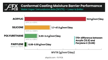
| Coating Type | Best For | Operating Range | WVTR (g·mm/m²·day) |
|---|---|---|---|
| Acrylic | Moderate humidity, easy rework | -65°C to 125°C | 13.9 |
| Silicone | Thermal cycling, wide temp range | -65°C to 200°C | 1.7–47.5 |
| Polyurethane | Chemical / industrial / coastal | -40°C to 130°C | 0.93–3.4 |
| Parylene | Medical, aerospace, severe environments | -200°C to 200°C | 0.08–0.59 |
The WVTR (water vapor transmission rate) difference between acrylic and Parylene is staggering—Parylene C transmits 0.08 g·mm/m²·day versus acrylic's 13.9. For submersion-adjacent or high-humidity environments, standard coatings don't offer equivalent protection.
SFX PCB's conformal coating process covers the full application stack:
- Application methods: Automated spray, dip, brush, and selective robotic systems
- Standard dry film thickness: 25–40 μm
- Parylene nano-vacuum coating: Controllable between 5–30 μm via CVD
- Pre-coating prep: Deep solvent cleaning + pre-bake at 60°C for 30–40 minutes to eliminate trapped moisture and residual flux
SFX PCB's Parylene process uses vacuum vapor deposition (CVD) to create a pinhole-free barrier rated to IPX-8 protection, suitable for medical, aerospace, military, and marine applications.
Surface Finishes: Protecting Exposed Copper
| Finish | Corrosion Resistance | Harsh Environment Suitability |
|---|---|---|
| ENIG | Excellent | Preferred for most harsh environments |
| ENEPIG | Excellent (no black pad risk) | Best for wire bonding and demanding soldering |
| Hard Gold | Superior wear resistance | Connector contacts with repeated mating cycles |
| Immersion Silver/Tin | Moderate | Limited harsh environment use |
| OSP | Temporary only | Unsuitable for high-humidity deployments |
| HASL | Lowest | Not recommended for corrosive environments |
For most harsh-environment builds, ENIG is the default recommendation. ENEPIG offers advantages for applications where black pad risk is a concern. Hard gold plating is the right choice where connector contacts will see repeated insertion cycles—wear resistance matters more than solderability in that case.
Design and Manufacturing Practices That Reinforce Material Reliability
Material selection sets your performance limits. Design decisions determine how close you get to them.
Copper Weight and Thermal Via Strategy
Increasing copper weight from 1 oz to 2 oz or higher delivers three simultaneous benefits:
- Higher current-carrying capacity without thermal penalties
- Lower thermal resistance through the trace stack
- Greater mechanical strength against vibration-induced trace cracking
SFX PCB supports copper weights from standard 1 oz up to 20 oz for heavy copper builds, with design constraints that scale accordingly (6/8 mil line/space at 3 oz, 12/12 mil at 6 oz). Thermal via arrays beneath high-power components channel heat through the board stack efficiently—a design technique that costs nothing in material but directly extends component lifespan.
Component Placement for Mechanical Resilience
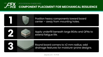
Three placement rules that reduce substrate stress in vibration environments:
- Position heavy components toward board center, away from mounting holes where bending stress concentrates during shock events
- Apply underfill or adhesive beneath large BGAs and QFNs — fatigue life increases substantially with proper underfill elastic modulus
- Round board corners to ≥ 2 mm radius and include drainage features in moisture-prone designs
DFM Analysis Before Fabrication
Catching material-reliability risks before fabrication is far cheaper than discovering them in qualification testing. SFX PCB's free DFM analysis with every order surfaces common issues, including:
- Insufficient trace spacing for the target laminate
- Annular ring problems that compromise via integrity
- Stack-up configurations mismatched to the substrate's thermal properties
For harsh-environment builds, DFM review of controlled-impedance geometries under the thermal characteristics of the chosen laminate is particularly valuable. Impedance drift that passes simulation at room temperature can exceed spec at actual operating temperature — catching this before fab prevents costly respins.
Testing and Qualifying Your PCB for Harsh Environment Deployment
Material and design choices must be validated experimentally. These are the key qualification tests and what each proves:
| Test | Standard | What It Validates |
|---|---|---|
| Thermal Cycling | IPC-9701A / MIL-STD-883 Method 1011 | CTE mismatch failures, solder joint integrity |
| Humidity/Moisture | IPC-TM-650 2.6.3F (85–93% RH) | Coating and substrate moisture resistance |
| Salt Spray | MIL-STD-202 / IPC-TM-650 | Surface finish and coating corrosion resistance |
| Vibration & Shock | MIL-STD-810H / IPC-9701A | Solder joint and mechanical integrity |
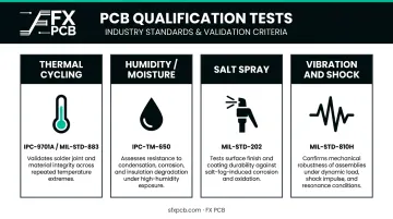
SFX PCB performs thermal cycling, humidity exposure, vibration testing, and accelerated life testing alongside 100% electrical testing on all bare boards.
Failure Analysis Methods
When post-test failures occur, understanding the failure mode informs design corrections:
- Optical inspection — surface defects and corrosion
- Microsection analysis — via barrel integrity and lamination quality
- X-ray inspection — hidden solder joint failures beneath BGAs
- SEM/EDX — chemical composition of corrosion products or contamination
IPC Class 2 vs. Class 3
| IPC Class 2 | IPC Class 3 | |
|---|---|---|
| Applications | Industrial electronics, commercial products | Aerospace, military, medical life-support |
| Downtime tolerance | Occasional downtime acceptable | Zero tolerance for failure |
| Requirements | Standard tolerances and inspection | Tighter tolerances, rigorous inspection, comprehensive stage-by-stage testing |
Specifying the correct class at the design stage drives material and process decisions throughout production. SFX PCB is certified to IPC-A-610 Class 2 and Class 3, with ISO 13485 certification covering medical-grade manufacturing requirements.
Frequently Asked Questions
What is a reliability test for PCB?
PCB reliability testing exposes a board or assembly to controlled stressors—thermal cycling, humidity, vibration, chemical exposure—to verify performance across its intended service life. Test procedures follow standards including IPC-TM-650, MIL-STD-810H, and IPC-9701A, conducted at both the bare-board fabrication stage and finished-assembly level.
What is the lifespan of a PCB?
Lifespan depends on environment, material selection, and protective measures. Well-designed PCBs in benign indoor conditions can last 20+ years. In harsh environments without proper material hardening, failures can occur within 6–18 months. Boards engineered for extreme conditions—high-Tg substrates, conformal coatings, robust surface finishes—reliably achieve 5–10+ year field lifespans.
Which PCB substrate material is best for high-temperature environments?
The right choice depends on your temperature range and application:
- High-Tg FR-4 (Tg ≥ 170°C) — handles most industrial and automotive needs
- Polyimide (Tg ~250°C) — suited for aerospace and military applications
- PTFE laminates — preferred when high-frequency stability at elevated temperatures is also required
- Metal-core substrates — best when heat dissipation is the primary challenge
What is conformal coating, and when is it required?
Conformal coating is a thin protective polymer film applied to an assembled PCB to guard against moisture, dust, chemicals, and corrosion. It's required—or strongly recommended—for boards exposed to humidity above ~65% RH, chemical environments, outdoor conditions, or applications in automotive, marine, medical, and aerospace sectors.
What is the difference between IPC Class 2 and Class 3 for harsh environment PCBs?
IPC Class 2 covers general industrial electronics where extended service life matters but occasional downtime is acceptable. IPC Class 3 applies to mission-critical applications—aerospace, military, medical life-support—where failure cannot be tolerated, requiring tighter manufacturing tolerances and stricter acceptance criteria throughout fabrication and assembly.