Telecom PCB Fabrication
Manufacture rigid, multilayer, metal-based, high-frequency, and rigid-flex boards built for telecom signal integrity, thermal stability, and scalable production with fine-line capability and tested surface finishes.
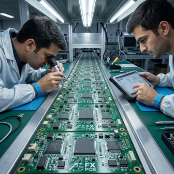
Build reliable telecom hardware with FX PCB’s integrated PCB fabrication and assembly services. From high-frequency boards and dense multilayer designs to turnkey SMT/THT assembly, testing, and compliant finishing, we help network equipment teams reduce risk, shorten development cycles, and move confidently from prototype to production. Backed by certified processes and global support, every build is engineered for signal integrity, durability, and repeatable performance.
End-to-end PCB fabrication, assembly, sourcing, and testing built for telecom reliability, speed, and production scalability.
Manufacture rigid, multilayer, metal-based, high-frequency, and rigid-flex boards built for telecom signal integrity, thermal stability, and scalable production with fine-line capability and tested surface finishes.
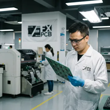
Transform telecom PCB designs into production-ready assemblies using SMT, through-hole, and mixed-technology processes supported by AOI, X-ray inspection, functional testing, and IPC-standard quality controls.
Streamline your build with component sourcing, procurement, assembly, testing, programming, and final inspection handled under one coordinated turnkey workflow for faster telecom product launches.
Validate new telecom designs quickly with small-batch prototype assembly built to your Gerber files and BOM, helping teams debug, iterate, and reduce costly redesign cycles.
Accelerate urgent telecom development schedules with fast PCB assembly, smart part replacement suggestions, and transparent project communication while maintaining precision, inspection, and quality standards.
Verify assembled telecom boards with custom functional test jigs, electrical checks, performance validation, and configuration procedures developed around your specific operating requirements.
Every project begins with a free DFM analysis to identify manufacturability risks, layout concerns, tolerance issues, and material considerations before production. For telecom boards, stackup planning supports signal integrity, impedance control, and reliable multilayer performance.
Partner with a certified PCB and PCBA manufacturer built for demanding telecom programs.
ISO9001, ISO14001, ISO13485, and IPC-A-610 Class 2/3 standards support consistent production.
Prototype assemblies can begin from 24 hours once all required parts are available.
Smart procurement and 600k+ local stock access help mitigate shortages and control costs.
Move from bare PCB fabrication to turnkey assembly, testing, coating, and scale-up seamlessly.
Experienced engineers supporting telecom PCB programs from prototype through production.
FX PCB has spent more than 15 years building its reputation as a full-service PCB and PCBA manufacturing partner for demanding industries, including Telecommunications, Medical Devices, Automotive, Industrial Automation, and Consumer Electronics. The company operates dedicated PCB and PCBA facilities in Shenzhen, China, with a US office in Plano, Texas to support North American clients more directly. What began as PCB fabrication has evolved into a complete electronics manufacturing solution covering DFM review, component sourcing, assembly, inspection, functional testing, and compliant finishing. FX PCB’s mission is to help clients bridge the gap between innovative concepts and market-ready products through reliable quality, speed to market, collaborative support, and continuous manufacturing improvement.
Telecom PCBs often require tighter control of signal integrity, impedance, thermal performance, and long-term reliability than general-purpose electronics. Designs may include high-frequency materials, dense multilayer stackups, fine traces, and strict inspection needs. FX PCB supports telecom builds with DFM review, advanced fabrication capabilities, SMT/THT assembly, AOI, X-ray, electrical testing, and IPC-A-610 Class 2/3 quality practices.
Send your files and requirements for expert manufacturing guidance.

Quality management for consistent PCB manufacturing.
Assembly workmanship standard for reliable electronics.

Recognized safety compliance for electronic products.
Share your Gerber files, BOM, quantity, and testing requirements. FX PCB will review your project, identify manufacturability considerations, and provide a clear path from quote to production.
For immediate assistance, feel free to give us a direct call at (+1) 5103455000. You can also send us a quick email at info@sfxpcb.com.
For immediate assistance, feel free to give us a direct call at (+1) 5103455000. You can also send us a quick email at info@sfxpcb.com.