Layout Optimization
We support dense, performance-critical PCB layouts with attention to routing strategy, stackup feasibility, impedance control, and manufacturability so high-speed designs can move confidently toward fabrication.

Accelerate complex electronics with high-speed PCB design and layout support built for reliable signal integrity, controlled impedance, and manufacturable results. FX PCB helps engineering teams move from concept to production with DFM insight, advanced fabrication capabilities, and assembly expertise for demanding medical, automotive, industrial, telecom, and consumer electronics applications worldwide without costly late-stage redesigns or sourcing delays.
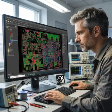
End-to-end support for complex PCB layouts, manufacturability, prototyping, testing, and production-ready electronic assemblies.
We support dense, performance-critical PCB layouts with attention to routing strategy, stackup feasibility, impedance control, and manufacturability so high-speed designs can move confidently toward fabrication.
Every order can benefit from free DFM review to catch fabrication, assembly, spacing, drill, and component issues early, helping prevent expensive rework before boards are released.
FX PCB manufactures advanced boards including high-frequency, multilayer, rigid-flex, metal-based, ceramic, and glass PCBs with fine line widths, laser drilling, and multiple surface finishes.
Prototype PCB Assembly helps validate high-speed designs quickly with SMT and THT assembly, flexible part sourcing, professional build quality, and practical support for testing and iteration.
Our experienced sourcing team uses access to over 600k local stock, alternative part suggestions, and customer-approved substitutions to reduce lead times and supply chain risk.
PCBA Functional Testing verifies electrical performance using custom test procedures, fixtures, jigs, and configuration checks aligned to your application requirements and production expectations.
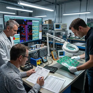
We begin by reviewing your Gerbers, BOM, stackup needs, performance goals, and application constraints. This helps our engineering team identify critical nets, manufacturing risks, component concerns, and assembly requirements before production planning begins.
FX PCB combines engineering support, direct manufacturing, and quality systems for demanding PCB projects.
ISO-certified facilities follow IPC-A-610 Class 2/3 standards for dependable electronic assemblies.
Prototype builds can start quickly once parts are available, reducing development delays.
Move from prototype to mass production with one experienced PCB and PCBA partner.
Facilities in Shenzhen and a Plano office support customers across worldwide markets.
Experienced PCB specialists supporting complex electronics from concept to production.
FX PCB has built its reputation over more than 15 years in PCB and PCBA manufacturing, growing from a fabrication provider into a comprehensive electronics manufacturing partner. With dedicated PCB and PCBA factories in Shenzhen and a US office in Plano, Texas, the team supports customers across North America and global markets with responsive communication and direct manufacturing access. The company serves demanding industries including medical devices, automotive, industrial automation, telecommunications, aerospace, defense, and consumer electronics. Its mission is to help clients turn innovative concepts into reliable, market-ready products through uncompromising quality, speed to market, collaborative partnership, environmental responsibility, and continuous innovation.
High-speed PCB design is usually defined less by clock frequency alone and more by signal rise time, trace length, impedance, and timing sensitivity. A board becomes high-speed when interconnects behave like transmission lines, requiring controlled impedance, return-path planning, length matching, crosstalk control, and careful stackup design to preserve signal integrity.
Talk with FX PCB about files, timelines, sourcing, and testing.

Quality management for consistent PCB production
Assembly standards for reliable electronic products

Recognized compliance support for global markets
Send your design files, BOM, timeline, and testing needs. FX PCB will review your project and help plan a manufacturable path from prototype to production.
For immediate assistance, feel free to give us a direct call at (+1) 5103455000. You can also send us a quick email at info@sfxpcb.com.
For immediate assistance, feel free to give us a direct call at (+1) 5103455000. You can also send us a quick email at info@sfxpcb.com.