Introduction
Ceramic PCBs are built on rigid, inorganic substrates using high-temperature bonding, vacuum deposition, or precision printing techniques that share almost nothing with standard FR-4 production. Where FR-4 relies on laminating glass-fiber epoxy and etching pre-clad copper, ceramic fabrication must create or bond a metal layer directly to a surface with no inherent adhesion.
The two substrate families exist in different engineering categories entirely.
The gap in thermal performance alone tells part of the story: FR-4 laminates like Isola FR408 deliver roughly 0.4 W/m·K in thermal conductivity, while aluminum nitride ceramic substrates reach 150–240 W/m·K. That's a 375–600× difference — enough to determine whether a power module runs within spec or fails under load.
This guide is written for engineers and technical buyers in power electronics, automotive, aerospace, medical devices, and telecom. It covers what actually happens inside the factory: how each process works, why method selection affects yield and cost, and where things go wrong.
Key Takeaways
- Ceramic PCB manufacturing uses six metallization methods: HTCC, LTCC, DBC, DPC, thick film, and AMB — each suited to different performance tiers and cost targets
- Substrate material (alumina, AlN, or Si₃N₄) and metallization method together set thermal conductivity, trace resolution, CTE match, and operating range
- DPC delivers trace resolutions down to 50 µm, while DBC and AMB handle high current loads with thick copper layers
- Process selection follows application requirements: line width, current capacity, thermal load, and temperature range
- Standard QC includes AOI, X-ray void inspection, electrical testing, and thermal cycling validation — skip any of these at your own risk
What Is Ceramic PCB Manufacturing?
Ceramic PCB manufacturing is the process of forming conductive circuit layers on a rigid inorganic ceramic substrate using high-temperature bonding, vacuum deposition, or screen-printing techniques — not conventional lamination.
The intended result is a board that sustains operation under high thermal load, high voltage, and extreme environmental conditions without the degradation that polymer substrates accumulate over time.
The table below shows how ceramic fabrication differs from standard FR-4 across the attributes that matter most in high-performance applications:
| Attribute | FR-4 PCB | Ceramic PCB |
|---|---|---|
| Substrate | Glass-fiber epoxy laminate | Alumina, AlN, or Si₃N₄ |
| Copper bonding | Etches pre-clad copper foil | Bonds or deposits metal onto non-adhesive ceramic |
| Max thermal conductivity | ~0.4 W/m·K | 22–240 W/m·K depending on substrate |
| Process temperature | 130–180°C | 800–1,650°C depending on method |
| Trace resolution | Moderate | Varies: 50 µm (DPC) to wider for DBC/AMB |
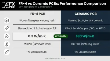
FR-4 fabrication works because the substrate already arrives copper-clad. Ceramic fabrication must create that bond from nothing — against a surface with no natural affinity for metal adhesion, and across a CTE mismatch that stresses that bond with every thermal cycle.
Why Ceramic PCB Manufacturing Requires a Fundamentally Different Approach
The Core Material Challenge
Ceramic substrates arrive without copper cladding, without resin, and without any compatibility with standard wet lamination. Every metallization step has to account for two problems simultaneously: achieving strong adhesion to an inert ceramic surface, and managing the thermal expansion mismatch between ceramic and metal.
Per MARUWA's published data for Si₃N₄, silicon nitride has a CTE of 2.6 × 10⁻⁶/K — closely matching silicon's ~2.6 × 10⁻⁶/°C. Alumina sits at 8.2 × 10⁻⁶/°C. Across thousands of thermal cycles per year in a power module, that difference accumulates into solder joint fatigue and eventual delamination.
What High-Performance Applications Demand
The complexity exists because the application requirements are genuinely extreme:
- Thermal conductivity 375–600× higher than FR-4
- Operating temperatures exceeding 200°C continuously
- CTE values matched to silicon dies to prevent solder joint fatigue
- Dielectric stability at GHz frequencies (AlN grades show dielectric constants of 8.4–8.6 at 2 GHz per Kyocera's published specifications)
No organic substrate reliably meets all four simultaneously.
Where FR-4 Assumptions Break Down
Meeting those requirements demands process assumptions that don't exist in standard FR-4 workflows. Engineers who carry over FR-4 design habits to ceramic projects encounter well-documented failure modes:
- Applying standard trace width calculations to thick copper layers on DBC substrates
- Specifying sintering temperatures without accounting for atmosphere control
- Selecting a metallization method incompatible with the required via geometry
Each of these leads to delamination, poor adhesion, or thermal failure — typically discovered after fabrication, not before.
How the Ceramic PCB Manufacturing Process Works
Ceramic PCB manufacturing follows a four-phase sequence: substrate preparation → metallization → via formation and layer stacking → surface finishing and quality control.
Phase 1: Substrate Preparation
Incoming ceramic sheets — alumina, AlN, or Si₃N₄ — are inspected for dimensional accuracy and surface defects, then cleaned via ultrasonic baths or plasma etching to achieve the nanoscale surface flatness required for reliable metal adhesion.
Substrate selection at this stage determines the performance ceiling:
- Alumina (Al₂O₃): 22–33 W/m·K thermal conductivity depending on purity grade (CoorsTek AD-96 at 24.7 W/m·K vs. AD-995 at 30.0 W/m·K); best cost-performance balance for most applications
- Aluminum nitride (AlN): 150–240 W/m·K per Kyocera's published grades; chosen when maximum heat dissipation is required
- Silicon nitride (Si₃N₄): 85 W/m·K with bending strength of 800 MPa and fracture toughness of 6.5 MPa·√m per MARUWA's SN-90 data; preferred where thermal cycling resistance and CTE match to silicon are the primary concerns
Purity grade matters beyond thermal conductivity. CoorsTek's alumina data shows dielectric loss improving from 0.0004 at 96% purity to below 0.0001 at 99.5%+ grades — directly affecting high-frequency performance.
Phase 2: Metallization and Circuit Layer Formation
The metallization method chosen here defines trace resolution, operating temperature range, current-carrying capacity, and cost. Six methods are in commercial use — the table below summarizes the key trade-offs:
| Method | Firing Temp | Trace Resolution | Max Cu Thickness | Best For |
|---|---|---|---|---|
| HTCC | ~1,600°C | Coarse (W/Mo paste) | ~15 µm | Structural strength; hermetic packaging |
| LTCC | 870–880°C | Medium (Ag/Au paste) | ~15 µm | 3D multilayer; embedded passives |
| DBC | ~1,065°C | Wide traces only | 200–600 µm | High-current power modules; batch cost efficiency |
| DPC | Room temp (sputter) | 50 µm line-space | 100–150 µm | Fine-pitch circuits; optical and RF modules |
| Thick Film | ~850°C | Coarser than DPC | ~15 µm | Multilayer hybrids; resistor printing |
| AMB | 800–1,000°C | Medium | Up to 800 µm | Si₃N₄ power modules; extreme thermal cycling |
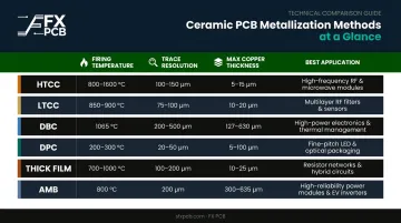
A few methods warrant additional detail:
DBC bonds copper foil directly to ceramic in a controlled nitrogen/oxygen atmosphere, exploiting the copper-oxygen eutectic reaction to form an oxide bond layer. Rogers curamik DBC substrates use copper layers of 200–600 µm — making it the most cost-efficient choice for batch production, though it requires wider trace widths.
DPC sputters a titanium adhesion seed layer (50–100 nm) onto ceramic in vacuum, then builds copper to 100–150 µm via electroplating. Photolithography defines the circuit pattern. Per the IMAPS DPC technical paper, this achieves 50 µm line-space resolution with 20 µm minimum tolerance — the finest resolution of any ceramic metallization method. SFX PCB uses DPC as its primary ceramic process, supporting trace widths down to 0.075 mm on Al₂O₃ and AlN substrates.
AMB bonds copper to ceramic using a titanium-bearing active solder in a vacuum brazing furnace at 800–1,000°C. The titanium reacts with the ceramic surface to create a wettable interface. Rogers confirms AMB can reach 800 µm copper thickness — the thickest option available — making it the standard choice for Si₃N₄ substrates in demanding power module applications.
Phase 3: Via Formation and Layer Stacking
Via formation method depends on process stage:
- Green-state punching: Used in HTCC and LTCC before firing; enables complex via geometries at lower cost
- Laser drilling: Used on fired substrates in DPC and thin-film processes; achieves precision micro-via diameters (SFX PCB supports minimum PTH via diameters of 0.06 mm)
- Via fill: Conductive paste fill or copper plating, co-fired or plated in subsequent steps
Layer stacking differs by process: HTCC and LTCC stack and laminate individual printed layers before final co-firing, while DPC and thick film deposit dielectric layers between conductive layers and fire sequentially. In both cases, differential shrinkage between layers is the primary process risk. Mismatched shrinkage rates cause dimensional deviation and delamination — which is why validated, substrate-specific firing profiles are essential, not optional.
Phase 4: Surface Finishing and Quality Control
After metallization, surface finishing protects traces and prepares the board for component attachment. SFX PCB offers three options for ceramic PCBs:
- ENIG — electroless nickel/immersion gold; standard for solderability and wire bondability
- ENEPIG — adds palladium layer for enhanced die attach and wire bonding performance
- Immersion Silver — cost-effective alternative with good solderability
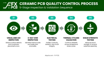
Quality control follows a structured sequence:
- Visual and AOI inspection post-sintering for surface defects
- X-ray inspection to detect internal voids between metal and ceramic layers (the IMAPS DPC paper notes DBC substrates commonly show 5–10% void distribution between ceramic and copper — a process control benchmark, not an acceptance specification)
- Electrical testing for continuity and insulation resistance — SFX PCB applies 100% electrical testing before shipment on all ceramic boards
- Thermal cycling validation to confirm bond integrity under repeated temperature stress
- Shear strength testing to verify metal-ceramic adhesion meets specification
SFX PCB holds ISO 9001, ISO 13485, and IPC-A-610 Class 2/3 certifications, covering ceramic PCB production for medical, automotive, and industrial applications.
Key Factors That Affect Ceramic PCB Manufacturing Outcomes
Substrate Purity Grade
The gap between 96% and 99.5% alumina is measurable: CoorsTek's data shows thermal conductivity rising from 24.7 W/m·K (AD-96) to 30.0 W/m·K (AD-995), while dielectric loss drops from 0.0004 to below 0.0001. Mismatched purity grades for the intended thermal or frequency requirement are a leading cause of premature board failure.
Metallization Method vs. Design Requirements
This is where most process mismatches originate:
| Method | Trace Resolution | Copper Thickness | Best For |
|---|---|---|---|
| DPC | 50 µm (20 µm tolerance) | 100–150 µm | Fine-pitch, precision packaging |
| DBC | ≥150 µm minimum | 200–600 µm | High-current power substrates |
| AMB | ≥200 µm minimum | Up to 800 µm | Power modules, Si₃N₄ substrates |
| Thick Film | ~60 µm+ | Thinner layers | Multilayer, embedded resistors |
Choosing the wrong method for your minimum feature size locks in fabrication constraints that no amount of process tuning can fix. SFX PCB's engineering team provides free DFM analysis on every ceramic PCB order, flagging trace-width and via-fill compatibility issues before fabrication starts and preventing costly respins.
Firing Temperature and Atmosphere Control
Sintering atmosphere (nitrogen for DBC, high vacuum for DPC and AMB), temperature ramp rates, and hold times require tight control. Deviations produce incomplete bonding, warpage from differential shrinkage, or metal layer oxidation. The Heraeus LTCC profile specifies 5°C/min ramp rates because faster ramp rates build the thermal stress gradients that cause microcracking in the ceramic substrate.
CTE Mismatch Management
When ceramic CTE doesn't match the semiconductor die or solder, repeated thermal cycling induces fatigue cracking at solder joints. Substrate selection is the primary tool:
- Si₃N₄: CTE 2.6 ppm/K — closest match to silicon
- AlN: CTE 4.6–4.8 ppm/K — moderate mismatch
- Al₂O₃: CTE 8.2 ppm/K — highest mismatch among these substrates
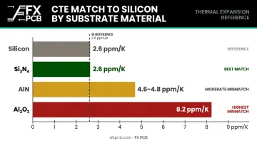
Metallization thickness directly influences stress distribution: thicker copper layers redistribute thermal stress but must be accounted for in the DFM review.
Common Misconceptions About Ceramic PCB Manufacturing
"All Ceramic PCBs Are Made the Same Way"
There are at least six distinct processes — each with different temperature ranges, conductor materials, resolution limits, and application fits. Specifying a "ceramic PCB" without defining the metallization method leaves the manufacturer guessing. Engineers should identify HTCC, LTCC, DBC, DPC, thick film, or AMB at the design stage.
"Ceramic PCBs Can't Achieve Fine Traces"
DPC achieves trace widths below 50 µm — finer than many standard FR-4 processes. This limitation applies specifically to DBC and AMB due to etching constraints, but engineers frequently and incorrectly generalize it to the entire ceramic PCB category. The result: boards get over-specified or ceramic substrates get ruled out entirely for precision applications where DPC would work well.
That trace-width confusion is process-specific. A separate — and equally common — misunderstanding involves the sintering step itself.
"Higher Sintering Temperature Always Means Better Bonding"
Excessive or uncontrolled temperatures cause warpage, ceramic grain growth, and metal layer oxidation. Effective ceramic PCB manufacturing is as much about controlling ramp rates, hold times, furnace atmosphere, and cool-down profiles as it is about hitting a target temperature. Manufacturers with calibrated kilns and validated firing profiles produce measurably fewer warped and delaminated boards than those running generic high-temperature parameters.
Frequently Asked Questions
How is a ceramic PCB manufactured step by step?
The core sequence: substrate preparation and surface cleaning, metallization via one of six methods (HTCC, LTCC, DBC, DPC, thick film, or AMB) depending on design requirements, via formation by punching or laser drilling, multilayer stacking where applicable, surface finishing (ENIG, ENEPIG, or immersion silver), and quality inspection covering AOI, X-ray, electrical testing, and thermal cycling validation.
How much does a ceramic PCB cost?
Ceramic PCBs cost significantly more than FR-4 because of high-purity substrate materials, specialized equipment (vacuum chambers, high-temperature kilns), and lower production volumes. DBC is the most cost-efficient method for batch production; DPC and AMB carry higher equipment costs, and AlN substrates add cost over alumina. Layer count and order volume are the primary pricing variables.
What is the difference between HTCC and LTCC ceramic PCBs?
HTCC fires at high temperatures using tungsten or molybdenum conductors, producing boards with strong structural integrity for extreme-heat environments. LTCC fires at approximately 870–900°C using silver or gold conductors, enabling passive component embedding and 3D multilayer designs — better suited for high-frequency communications where conductor resistivity and integration density matter more than peak temperature resistance.
Which ceramic PCB manufacturing method is best for high-power applications?
DBC and AMB are the preferred methods for high-power applications (IGBT modules, power converters, EV inverters) because both support thick copper layers with high current capacity. AMB is increasingly specified over DBC for silicon nitride substrates where thermal cycling resistance is critical — Si₃N₄'s CTE closely matches silicon and its mechanical toughness outperforms alumina.
Can ceramic PCBs support multilayer designs?
LTCC and HTCC both support true multilayer co-fired designs with embedded passives between layers. Thick film achieves multilayer structures through sequential printing and firing cycles. DPC and DBC are generally limited to single and double-sided configurations, though advanced DPC techniques enable some three-dimensional routing.
What substrate material should I choose for my ceramic PCB?
Alumina (Al₂O₃) offers the best cost-performance balance for most applications. AlN is the choice when maximum thermal conductivity is required (150–240 W/m·K) for high-power or RF designs. Silicon nitride (Si₃N₄) is selected for severe thermal cycling environments — its CTE of 2.6 × 10⁻⁶/K closely matches silicon, reducing solder joint fatigue in power modules.