The problem isn't the term itself. It's that engineers frequently specify, source, or evaluate boards against a vague idea of "high performance" rather than a precise set of measurable parameters. The result: boards that look correct on paper but fail in the field through signal degradation, thermal fatigue, or dielectric drift.
This guide defines high performance in technical terms — what properties determine it, how they interact, what happens when they're exceeded, and how to validate that a fabricated board actually meets the specification before it reaches assembly.
Key Takeaways
- High-performance PCBs are defined by controlled impedance, dielectric properties (Dk/Df), thermal stability (Tg/CTE), and signal integrity — not any single specification
- Common impedance targets are 50Ω single-ended and 100Ω differential, with ±10% tolerance as a standard fabrication threshold
- Datasheet values for Dk, Df, and Tg reflect lab conditions — actual field performance shifts with temperature, humidity, and aging
- Exceeding performance boundaries leads to progressive signal degradation, via fatigue, and compliance failures
- Independent validation — TDR, AOI, X-ray, and DFM review — separates boards that meet spec from boards that merely appear to
What "High Performance" Actually Means in a PCB
High performance is a design condition, not a product tier.
A PCB qualifies as high performance when it's engineered to maintain signal integrity, dimensional stability, and reliable power delivery under demanding operating conditions.
That typically means signal frequencies where transmission-line behavior dominates, tight impedance tolerances, high layer counts, and substrate materials selected for specific electrical and thermal properties — not cost.
Two ways "high performance" functions in practice:
- Impedance targets, Dk/Df material specs, copper weight, and stackup architecture define it at the design stage
- Acceptable signal loss thresholds and stable material property ranges define it during operation
High-performance boards aren't simply "better" boards. They're optimized for specific conditions. Over-specifying a board for a low-frequency application wastes cost. Under-specifying one for a high-speed application produces silent failures: signal degradation and intermittent errors rather than an obvious catastrophic fault.
How High-Performance PCBs Differ from Standard PCBs
| Parameter | Standard PCB | High-Performance PCB |
|---|---|---|
| Impedance control | Not required | Required (±10% or tighter) |
| Substrate material | Standard FR-4 | High-Tg FR-4, Rogers, PTFE |
| Signal edge rates | Low-speed, tolerant | Fast edges, transmission-line sensitive |
| Design rules | Basic spacing/clearance | Differential pairs, return path management, via stub control |
| Validation | Visual / basic continuity | TDR, AOI, X-ray, coupon-based testing |
| Fabrication cost | Lower | Significantly higher |
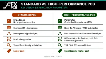
The design complexity gap matters practically: high-performance boards require stackup simulation, layer architecture engineering, and tighter fabrication tolerances that standard PCB workflows don't routinely apply. A manufacturer unfamiliar with controlled-impedance production will deliver boards that measure within visual tolerance but fail impedance targets.
Key Technical Properties That Define High-Performance PCBs
Signal integrity, thermal behavior, and dielectric characteristics are interdependent. Specifying one without understanding the others is where most design failures originate, and they're rarely obvious until after fabrication.
Signal Integrity and Impedance Control
Controlled impedance is the practice of designing trace geometry — width, spacing, dielectric thickness — to achieve a specified characteristic impedance so signals travel without reflections, ringing, or excessive loss.
Common targets: 50Ω for single-ended lines, 100Ω differential for high-speed interfaces like PCIe and HDMI, and 90Ω differential for USB 2.0. IPC technical testing uses ±10% TDR limits as the standard acceptance window.
Signal integrity also includes:
- Crosstalk — electromagnetic coupling between adjacent traces, worsened by inadequate spacing or missing return planes
- Return path continuity — high-speed signals must route over a solid ground reference; routing across plane splits increases series inductance and radiated emissions
- Via stub resonance — in multilayer boards, unused via barrel length acts as an unterminated transmission line; at sufficient frequencies, this creates a notch in frequency response that corrupts signals
Manufacturing tolerances directly shift realized impedance. Trace width variation from etch processes, dielectric thickness variation during lamination pressing, and copper surface roughness all push fabricated impedance away from design intent. These tolerances must be built into the impedance model at design time — not treated as acceptable post-fabrication variation.
Those same fabrication variables affect thermal performance too, which introduces the next set of material constraints.
Thermal Stability and Heat Dissipation
The glass transition temperature (Tg) is the point above which the substrate resin softens and z-axis thermal expansion increases sharply. Operating near or above Tg accelerates via fatigue and causes delamination under thermal cycling.
Material comparison:
| Material | Tg | Z-axis CTE (pre-Tg) |
|---|---|---|
| Isola DE104 (standard FR-4) | 135°C | 70 ppm/°C |
| Isola FR406 (high-Tg FR-4) | 170°C | 60 ppm/°C |
| Isola P95/P25 (polyimide) | 260°C | 55 ppm/°C |
| Rogers RO4003C | >280°C | 46 ppm/°C |
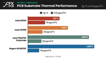
Beyond Tg, CTE mismatch between copper, substrate, and component packages drives cumulative mechanical fatigue — particularly in boards that see repeated thermal cycling. The substrate expands and contracts at a different rate than the copper and component leads, stressing via barrels and solder joints with each temperature excursion.
NASA's PCB reliability research identifies PTH/via circumferential cracking from cyclic fatigue as a primary failure mechanism in multilayer boards under repeated thermal cycling.
Dielectric Properties and Signal Loss
Thermal properties govern mechanical reliability; dielectric properties govern electrical performance at frequency. Two material values define how a board handles high-frequency signals:
- Dielectric constant (Dk) — determines signal propagation speed and directly affects impedance. An inconsistent Dk introduces phase distortion in wideband applications. Isola DE104 (standard FR-4) measures Dk 4.46 at 100 MHz, dropping to 4.32 at 5 GHz — not a fixed value.
- Dissipation factor (Df, or loss tangent) — determines how much electromagnetic energy the substrate absorbs. DE104 measures Df 0.022 at 1 GHz. Rogers RO4003C measures Df 0.0027 at 10 GHz. Rogers RT/duroid 5880 PTFE measures Df 0.0009 at 10 GHz — roughly 24× lower than standard FR-4.
As frequency rises, dielectric loss dominates signal attenuation. An IEEE 802.3 analysis of FR-4 found skin-effect and dielectric losses converging at around 205 MHz for a specific geometry — and loss compounds significantly above that point as channel length and data rate increase.
Moving to Rogers or PTFE-based laminates improves electrical performance, but it adds meaningful cost, extends lead times, and requires fabrication experience that not every manufacturer carries. Specifying these materials for designs well within FR-4's capable range is a common and expensive engineering mistake.
Factors That Affect PCB Performance in Real-World Operation
Material datasheets represent controlled laboratory conditions — typically 23°C and 50% relative humidity. Field operation is different in every dimension that matters.
Material Selection and Manufacturing Tolerances
Substrate selection is the most consequential design decision because it fixes Dk, Df, Tg, and CTE for the board's lifetime. Every other design choice operates within those material constraints.
Manufacturing tolerances then determine how close fabricated performance gets to designed performance:
- Trace width variation from etch processes shifts impedance
- Dielectric layer thickness deviation during lamination pressing shifts impedance
- Copper surface roughness increases insertion loss at high frequencies, with the effect growing as frequency rises and skin depth decreases
These aren't post-fabrication excuses — they're parameters that must be modeled into the impedance calculation before the board is built.
Operating Environment and Aging
Real boards face conditions that move performance away from design intent over time:
- Temperature — high duty cycles raise board temperature toward Tg, softening the substrate and accelerating mechanical fatigue
- Humidity — moisture absorption increases Dk and loss tangent; DE104 absorbs up to 0.3% moisture versus 0.02% for RT/duroid 5880, enough to shift dielectric properties at operating frequencies
- Thermal cycling — repeated temperature swings accumulate fatigue in via barrels and plated-through holes, causing boards that pass initial testing to fall out of spec in the field
- Copper oxidation — affects surface conductivity at high frequencies where signal energy concentrates at the conductor surface
An IPC study found that after thermal exposure, a phenolic-cure FR-4 material showed a Df increase of 35.1% at 75°C compared to room temperature. That magnitude of change directly alters signal loss calculations — it cannot be treated as minor variance.
Temperature and frequency stability requirements leave little room for material compromise in demanding applications. For 77 GHz automotive radar, Rogers RO4835 is specified for its enhanced stability at high temperatures and oxidation resistance — FR-4 simply cannot maintain consistent Dk and Df at those temperatures and frequencies.
How High-Performance PCBs Are Specified, Measured, and Validated
A stated impedance value on a schematic means nothing without a validated test result from the fabricated panel.
Specification and Documentation
Impedance specifications must appear in fabrication drawings or Gerber notes with:
- Explicit stackup definition (layer materials, thickness, copper weight)
- Dielectric constant assumptions at operating frequency
- Impedance targets and tolerance windows
IPC-2141A provides the design framework for controlled-impedance boards; IPC-A-610 governs assembly acceptance criteria. Both rated and tested values should be specified — they regularly diverge, and designs need margin to cover that gap.
Measurement and Validation Methods
| Method | What It Validates |
|---|---|
| TDR (Time Domain Reflectometry) | Impedance — injects a step pulse and derives Z0 from reflected amplitude, per IPC-TM-650 2.5.5.7A |
| AOI (Automated Optical Inspection) | Trace geometry, component placement, solder defects |
| X-ray inspection | Internal via integrity, BGA solder quality, hidden voids |
| Functional electrical testing | In-circuit performance against the full specification |
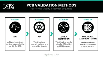
TDR specimens can be the board itself, nonfunctional lines built into the board, or coupons cut from the production panel. Coupon-based testing should be required in procurement documentation for any controlled-impedance build — it's the only way to verify fabricated impedance before assembly.
SFX PCB performs 100% electrical testing on every bare board as standard, alongside AOI and X-ray inspection, using flying probe testers. This verifies fabricated boards against specification before assembly begins — catching defects that visual inspection alone cannot detect.
Design for Manufacturability (DFM)
DFM analysis reviews the design against the manufacturer's fabrication capabilities before production begins — making it the most effective point to catch problems before tooling cost is committed. A thorough DFM review can:
- Confirm whether specified impedance is achievable within process tolerance
- Flag trace-spacing violations that would cause fabrication failures
- Recommend stackup adjustments to meet performance targets
SFX PCB provides free DFM analysis with every order, covering stackup review, impedance achievability, spacing validation, and geometry adjustments. This happens during the quotation stage, with findings communicated back to the customer for approval before production begins.
What Happens When Performance Limits Are Exceeded
Performance degradation in high-performance PCBs is rarely a binary failure. It builds progressively — from marginal signal quality to catastrophic failure or compliance violation — and the intermediate stages are often invisible without targeted test equipment.
Signal Degradation Mechanisms
Operating above the frequency ceiling for which a board was designed produces:
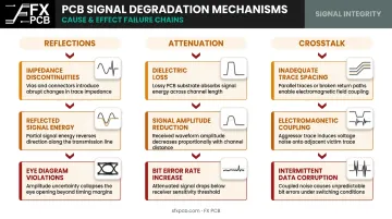
- Reflections from impedance discontinuities at vias, connectors, and trace transitions
- Signal attenuation from dielectric loss accumulating over channel length
- Crosstalk from inadequately spaced traces or broken return paths
At the system level, these manifest as elevated bit error rates, data corruption, or intermittent functional failures that engineers can only diagnose with signal integrity measurement. IEEE 802.3 identifies eye-diagram mask violations in amplitude or bit-time jitter as the direct path to unacceptable BER. It also notes that fabrication quality — including over-etching of differential pairs — directly affects the eye response.
Thermal and Material Failure
Operating near or above Tg softens the substrate, accelerating via fatigue and delamination under thermal cycling. CTE mismatch above Tg generates stress at solder joints and plated holes that accumulates into cracking. These are time-domain failures: they pass initial testing but surface in field service after repeated thermal excursions.
Compliance and Regulatory Consequences
Boards in medical, automotive, and aerospace applications must meet IPC Class 2 or Class 3 reliability standards. When thermal or signal failures occur, they don't just affect performance — they can void compliance certification entirely.
A Class I FDA recall of the Hamilton C6 ventilator was directly tied to a mechanical defect on a PCB from the PCB separating process — a defect that could cause the ventilator to stop ventilation. In automotive, ISO 26262 functional safety requirements tie system-level safety ratings to component reliability, meaning a board failure can invalidate the entire safety case.
The downstream exposure includes:
- FDA recalls for medical devices where PCB defects affect patient safety
- ISO 26262 safety case invalidation for automotive systems tied to component reliability
- Field service liability when failures occur outside the lab after passing initial testing
Common Misconceptions About High-Performance PCB Specs
These five misconceptions appear consistently across high-performance PCB projects — and each one has caused real failures in production designs.
Treating nominal Dk as a fixed constant. Isola DE104 measures Dk 4.46 at 100 MHz and 4.32 at 5 GHz. Designing to a single assumed Dk across all frequencies will produce impedance that drifts more than predicted — generating failures that appear random but are entirely predictable.
Assuming high-Tg FR-4 is automatically low-loss. Isola FR406 improves thermal margin significantly with Tg 170°C, but still measures Df 0.0161 at 1 GHz and 0.0172 at 10 GHz. High-Tg and low-loss are separate properties — a material can have one without the other.
Ignoring interaction effects between parameters. Signal integrity, thermal performance, and dielectric behavior are coupled. Raising operating temperature shifts Dk, which shifts impedance, which affects signal integrity. Copper pours added for heat spreading also affect EMI and return path inductance. A thermal fix that introduces a signal integrity problem is a documented, real-world failure mode.
Applying datasheet values directly as field design targets. IPC-TM-650 conditions test specimens at 23°C and 50% RH. An industrial enclosure at 85°C junction temperature in humid conditions is a different environment entirely. Engineering practice requires worst-case analysis and derating before committing to a material — nominal datasheet values are a starting point, not a design target.
Over-specifying materials without understanding the trade-offs. Specifying Rogers or PTFE laminates for designs operating well within FR-4's capable frequency range adds cost, extends lead times, and introduces fabrication complexity with no performance benefit. Match material specification to actual operating requirements with appropriate margin — not to the most demanding theoretical case.
Frequently Asked Questions
How do high-performance PCBs differ from standard PCBs?
High-performance PCBs require controlled impedance, specialized low-loss substrates, and tighter design rules — differential pair routing, via stub management, and return path planning — plus rigorous validation like TDR and coupon-based testing. Standard PCBs don't require any of these. The distinction is driven by signal frequencies and reliability requirements, not vendor classification.
What is the difference between PWB and PWA?
PWB (Printed Wiring Board) refers to the bare board substrate with copper traces before any components are mounted — equivalent to the more commonly used term PCB. PWA (Printed Wiring Assembly) refers to the completed assembly with all electronic components soldered in place — equivalent to PCBA.
What does PCBA stand for?
PCBA stands for Printed Circuit Board Assembly — the fully assembled board with all components soldered and ready for integration into a final product. It's distinct from the bare PCB, which is the unpopulated substrate before assembly.
What materials are used in high-performance PCBs?
Common options include standard FR-4, high-Tg FR-4 (150–180°C), Rogers RO4003C/RO4350B for RF applications, PTFE-ceramic laminates for high-frequency designs, and polyimide for flexible or extreme-temperature use. Selection is driven by the application's Dk, Df, Tg, and CTE requirements, not a blanket preference for premium materials.
What is controlled impedance and why does it matter?
Controlled impedance means engineering trace geometry and stackup to hit a target characteristic impedance, commonly 50Ω single-ended or 100Ω differential. Without it, high-speed signals reflect at discontinuities, causing bit errors, signal distortion, and failures that are hard to diagnose once the board is built.
How does thermal management affect PCB performance?
When board temperature rises toward Tg, the substrate softens, CTE mismatch stress increases, vias crack, and dielectric properties drift — all of which degrade signal integrity and shorten board life. Thermal design needs to be built into material selection and stackup from the start, not retrofitted after the electrical design is finalized.