

The good news: most lead time delays are preventable. They trace back to specific, controllable decisions made during design, file preparation, and manufacturer selection — not to some fixed, immovable production schedule.
This article covers what actually drives PCB lead time, which design decisions compress it, how DFM review prevents the delays that catch most teams off guard, and how component sourcing can undermine an otherwise fast-turn plan.
Key Takeaways
- Simpler board configurations — fewer layers, through-hole vias, common surface finishes — directly reduce fabrication time
- DFM review before file submission eliminates the revision loops that cause most preventable delays
- Incomplete Gerber files and BOM mismatches are avoidable causes of 24–48 hour holds per round trip
- Choosing a manufacturer with local component stock and built-in DFM review can cut days off your timeline before production starts
What Actually Determines PCB Manufacturing Lead Time
Lead time isn't a single number. It's the cumulative total of sequential stages: design verification, material procurement, fabrication, assembly, and testing. A single hold at any stage pushes every downstream step back by the same margin.
Fabrication Time Varies Significantly by Board Type
PCBWay's published quick-turn data illustrates how layer count alone shifts timelines:
| Board Type | Standard Build | Urgent Option |
|---|---|---|
| 2/4 layer | 5 days | 48 hours |
| 6/8 layer | 7 days | 72 hours |
| 10+ layer | 10 days | 96 hours |
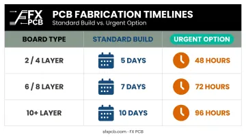
Assembly adds time on top of these figures — these are fabrication-only estimates. And if components need to be sourced, that happens in parallel with fabrication but can extend beyond it.
Design Complexity Is the Most Controllable Variable
Layer count, via type, copper weight, and trace/space tolerances each determine how many fabrication steps are required. More steps mean longer production windows. HDI designs with sequential lamination can reach 10–11 days for complex stackups, according to Sierra Circuits, and that's before assembly or shipping are factored in.
Queue Position and File Readiness Matter
Submitting incomplete files places your job on hold pending clarification. Each clarification request adds 24–48 hours. Ordering during peak production periods — without a complete, DFM-clean submission — puts you at the back of a longer queue.
Geography Affects End-to-End Delivery
Fabrication time and transit time are separate. DHL international delivery from Asia typically runs 3–7 business days on top of whatever the fab produces. A manufacturer with established US freight channels and a local US office can meaningfully shorten that end-to-end window. SFX PCB operates both Shenzhen factories and a US office in Plano, Texas, which supports North American logistics coordination.
Design Strategies That Directly Reduce Lead Time
The fastest way to shorten production time is to simplify the design before submitting files. Complexity added during layout translates directly into fabrication days.
Layer Count: Every Additional Layer Costs Time
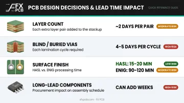
Two-layer and four-layer boards are significantly faster than six-layer-plus designs. Each additional layer adds lamination cycles, drilling operations, and inspection steps — the difference between a 4-layer and an 8-layer board on a standard build schedule is roughly two additional days. If routing efficiency can replace an extra layer through component placement optimization or differential pair routing, the time savings are immediate.
Via Selection Has a Bigger Impact Than Most Designers Expect
Through-hole vias are the fastest option — they require a single drilling and plating pass. Blind and buried vias require sequential lamination: the board is built in sub-assemblies, each drilled and etched independently before bonding. This process can add 4–5 days per additional lamination cycle.
Avoid blind/buried vias unless routing density genuinely requires them. Via-in-pad plated over (VIPPO) adds at least one additional day even on simpler boards.
Surface Finish Selection
Surface finish is another lever designers overlook. HASL and ENIG are the most widely supported finishes at most fabricators and don't require special process setup — making them the default choice for quick-turn orders.
Processing time varies noticeably between options:
- HASL: ~15–20 minutes processing time
- ENIG: ~90–120 minutes processing time
- Less common finishes: May require setup coordination outside a fast-turn queue
Stick with HASL or ENIG unless the application specifically demands otherwise.
Component Selection During Layout
A board ready in 48 hours still waits if one component is on a 6-week lead time. Address component availability during schematic capture, before files are ever submitted.
- Check BOM items against distributor stock before locking in the design
- Identify any single-source ICs, specialty FPGAs, or non-standard passives early
- Document approved alternates for critical parts before submission
SFX PCB's sourcing team proactively flags long-lead-time components during BOM review and will suggest qualified alternates — with customer approval required before any substitution is made.
Panel-Friendly Board Dimensions
Non-standard board sizes require custom tooling or V-score configurations. Boards that fit within standard panel dimensions (commonly 18" × 24" or 21" × 24") can often be panelized alongside other jobs, reducing setup overhead. Contact your manufacturer's engineering team during layout to confirm optimal dimensions for their production setup — catching this early avoids costly redesigns.
DFM Best Practices That Prevent Costly Delays
A board that fails DFM review after submission is placed on hold. Every day spent waiting for a designer response adds directly to the delivery date.
The Most Common DFM Issues That Cause Holds
Trace width and spacing: PCBWay lists 4 mil / 0.1 mm as the minimum manufacturable trace and spacing and strongly recommends designing above 6 mil / 0.15 mm. SFX PCB's stated minimum is 0.075 mm (approximately 3 mil), but designing at minimum capability is a risk flag — not a target. Run your CAD tool's DRC against the specific manufacturer's rule set, not just the software's default settings.
Annular ring sizes: Too-small annular rings create drilling breakout risk. Sierra Circuits notes that 2 mil clearance carries a 98% breakout probability, while 6–7 mil clearance reaches 0%. Design annular rings conservatively.
Solder mask clearance: Insufficient clearance around pads — typically below 4 mil — creates bridging risk during reflow. Silkscreen overlapping pads causes the same problem.
Copper balance: Uneven copper distribution across layers causes warping during lamination and reflow. Add copper pours or hatching on sparse layers to maintain balance. Poor copper distribution is a yield problem — unbalanced panels fail before they reach electrical test.
Run DFM Before You Submit
SFX PCB provides free DFM analysis for every order. Designers can submit files before committing to a full order and receive engineering feedback — typically within 12 hours — that identifies hold-triggering issues before they affect the production queue. This review catches the most common causes of multi-day delays without adding cost.
Matching your design tolerances to the fabricator's documented capabilities is what keeps boards moving through the queue on schedule.
Avoiding Hidden Delays: File Submission and Documentation
File errors cause more preventable production holds than any other single factor.
What Missing or Incorrect Files Actually Do
Each documentation error triggers a manual review hold and an email exchange. At 24–48 hours per round trip, two errors cost a full business week before production even starts.
The most frequent problems:
- Drill files, solder mask layers, and board outline (edge cuts) are frequently missing — Gerber format covers over 90% of PCB fabrication worldwide, and all layers must share identical coordinate systems
- Non-standard layer naming causes CAM software misreads, flagging files for manual review
- Excellon drill files without explicit decimal point specification are ambiguous and get held for clarification
- A single reference designator mismatch between BOM and pick-and-place file halts assembly completely
Generate Gerber files, BOM, and pick-and-place file from the same final schematic revision. Cross-check all three against each other before uploading — the checklist below covers exactly what to confirm.
The Five-Minute Pre-Submission Checklist
- Gerber package complete: all copper layers, solder mask (top and bottom), silkscreen, board outline, drill file
- Drill file format confirmed: Excellon with explicit decimal point specification, or Gerber X2 format
- BOM includes manufacturer part numbers and at least one approved alternate for critical components
- Pick-and-place file with correct component orientation data
- Fab notes included for controlled impedance: target impedance, tolerance, and relevant layers
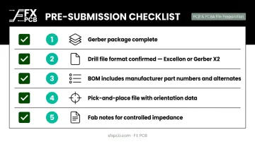
SFX PCB requires three files for turnkey PCBA: complete Gerber set, BOM in Excel format with manufacturer part numbers, and pick-and-place (centroid) file. Submitting all three simultaneously and correctly is the single most effective way to eliminate documentation-related delays.
Maintaining Quality Without Slowing Down
Fast turnaround and quality control aren't in opposition. The manufacturers that do both well build quality into the process rather than catching defects at the end.
End-of-line inspection after a full production run is slow and expensive. Upstream DFM review, incoming component verification, and automated in-process inspection are faster — and they prevent the more costly scenario of defects discovered post-assembly.
Three inspection methods keep quality tight without adding significant time:
- AOI (Automated Optical Inspection) scans for missing components, solder bridges, and misaligned parts at production line speeds, enabling 100% board coverage without adding significant time.
- X-ray inspection addresses what AOI can't see: BGA solder joints, hidden-joint voids, and inner-layer defects. For Class 3 applications (aerospace, defense, life-critical systems), tighter void limits and 3D laminography may apply; for Class 1 and 2, it's applied selectively based on component type and risk.
- Electrical testing on every bare board (a standard SFX PCB practice across prototype and production orders) catches connectivity issues before assembly begins — stopping defects at their cheapest point to fix.
SFX PCB is certified to IPC-A-610 Class 2 and Class 3, meaning acceptance criteria for solder joints, component placement, and workmanship are predefined for each application class. Predefined criteria mean inspectors apply consistent accept/reject standards rather than making judgment calls — fewer disputes, fewer revision cycles, and faster sign-off at delivery.
Frequently Asked Questions
How long does PCB manufacturing take?
Simple 2-layer rigid boards can be fabricated in as little as 24–48 hours on an urgent basis. Complex multilayer or flex designs typically run 7–14+ days. Assembly time is separate from fabrication, and component availability is often the actual schedule constraint on PCBA projects.
What are the four stages of PCB design?
The four core stages are:
- Schematic capture
- PCB layout and routing
- DFM and design rule checking
- Gerber/fabrication file generation
The quality of each stage determines whether manufacturing can begin without holds — particularly DFM review and file generation.
What factors matter most for high-speed PCB designs?
Three factors dominate: controlled impedance (typically 50 ohms, with ±10% standard tolerance or ±5% for precision), ground plane pairing to manage EMI, and material selection. FR-4 degrades above 5 GHz; specialty laminates like Rogers RO4350B are more stable at higher frequencies. Both impedance testing and specialty laminate procurement add lead time.
What is DFM and why does it matter for fast turnaround?
Design for Manufacturability is the practice of designing PCBs with production constraints built in. A DFM review before submission catches issues that would otherwise trigger manufacturing holds — the most common source of unexpected delays.
Can I really get a quality PCB assembled in 24 hours?
Yes — for simple designs. The three requirements are in-stock components, complete and DFM-clean files, and a manufacturer with dedicated fast-turn capacity. More complex boards or designs requiring component procurement will take longer.
What files do I need to submit to start manufacturing quickly?
Three files are required:
- Gerber package — all copper layers, solder mask, silkscreen, board outline, and drill file
- BOM — with manufacturer part numbers and approved alternates
- Pick-and-place file — for SMT assembly
Submitting all three simultaneously — and correctly — eliminates the most common source of production delays.