Introduction
Thermal management failure doesn't announce itself — it shows up six months after deployment as degraded LED output, a failed automotive control module, or a power converter running hot enough to shorten its own lifespan. In most of these cases, the root cause traces back to the PCB itself.
Metal Core PCBs (MCPCBs) solve this by replacing the standard fiberglass core with a metal substrate — typically aluminum or copper — that conducts heat away from components. Specifying an MCPCB, however, doesn't guarantee it's manufactured correctly.
Engineers, product designers, and procurement teams working on high-power LED lighting, automotive electronics, and power conversion systems frequently encounter this gap: the MCPCB manufacturing process is poorly understood at the operational level, particularly the via isolation and dielectric lamination steps that have no equivalent in standard FR4 fabrication.
A manufacturer without MCPCB-specific process controls will accept the order and deliver a board that looks right but fails under thermal load.
This guide covers the full manufacturing sequence — from metal base preparation through electrical testing — and flags the specific steps — dielectric bonding, via drilling, and surface finish — where shortcuts produce boards that pass visual inspection but degrade in the field.
Key Takeaways
- MCPCBs swap FR4 fiberglass for a metal base (aluminum, copper, or iron alloy) that provides structure, strength, and heat spreading in one layer
- Manufacturing follows 8 steps: base preparation → dielectric lamination → imaging → etching → via drilling/isolation → solder mask → surface finishing → electrical testing and profiling
- Via isolation (drill oversized hole → fill with epoxy → cure → re-drill → plate) has no FR4 equivalent and is the top source of field failures when skipped or rushed
- FR4 thermal conductivity is ~0.25 W/mK; aluminum bases reach 138–167 W/mK and copper reaches 386 W/mK — a measurable physics gap, not just a material preference
- MCPCBs are not universally superior: high-layer-count digital designs, complex signal routing, and low-power applications are often better served by FR4
What Is a Metal Core PCB and How Is It Structured?
An MCPCB — also called an Insulated Metal Substrate (IMS) PCB — bonds copper circuit layers to a metal plate through a thermally conductive dielectric layer. The metal plate, typically 1.0 mm to 3.2 mm thick, acts as the board's substrate, structural frame, and primary heat spreader simultaneously.
The Standard MCPCB Layer Stack
From top to bottom:
| Layer | Specification |
|---|---|
| Solder mask | Protective coating over copper traces |
| Copper circuit layer | 0.5 oz to 6 oz (35 µm to 210 µm) |
| Thermally conductive dielectric | 50–200 µm thick |
| Metal base | Aluminum, copper, or iron alloy |
The dielectric layer is the thermal bottleneck. Too thick and heat transfer degrades; too thin and electrical isolation fails. High-performance dielectrics like Ventec's VT-4B5H reach 4.2 W/mK, while Bergquist's HT-07006 operates at 2.2 W/mK — compared to FR4 prepreg, which typically falls below 0.5 W/mK.
Breakdown voltage ranges from 4,000 VAC at 50 µm to 12,000 VAC at 200 µm. That range lets designers trade off isolation strength against thermal conductivity based on their application requirements.
How Metal Bases Compare
- Aluminum 5052: 138 W/mK, cost-effective, most common
- Aluminum 6061: 167 W/mK, better for CNC machining and fastener applications
- Copper C1100: 386 W/mK, maximum thermal performance, higher cost and weight
A real-world consequence: NCAB's LED thermal comparison found maximum LED junction temperature at 129.1°C on FR4 versus 61.9°C on IMS — a 67°C reduction driven entirely by the substrate choice.
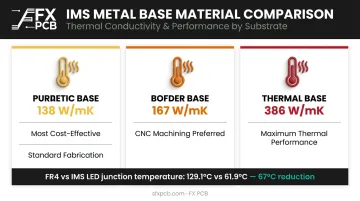
For applications where that thermal margin matters, SFX PCB manufactures aluminum, copper, and copper-aluminum composite base PCBs with board thicknesses from 0.5 mm to 5.0 mm and copper weights from 1 oz to 10 oz, covering the full range of thermal and power requirements.
Why MCPCB Manufacturing Requires a Specialized Process
The metal base creates a short-circuit risk that runs through every step of fabrication. Any process step that brings conductive materials into contact with the base without proper isolation produces a failed board.
What Goes Wrong Without MCPCB-Specific Controls
Three failure modes occur when standard FR4 processes are applied to MCPCBs without modification:
- Via drilling: In FR4, drill bits pass through non-conductive glass-epoxy. In MCPCBs, an uninsulated plated via wall touching the aluminum or copper core creates a direct short between circuit and ground — invisible until electrical testing, or only revealed when thermal cycling stresses the joint
- Dielectric lamination: Lamination profiles optimized for FR4 prepreg often fail to bond properly to smooth metal surfaces, creating interface voids that degrade thermal conductivity and trigger delamination under heat cycling
- Chemical etching: Etchants sized for standard copper removal can attack the metal base if the dielectric has pinholes or process parameters aren't adjusted for its thinner layer
These failure modes are well-documented. Bergquist's Thermal Clad guidance identifies micro-fractures, delaminations, and micro-voids as known risks, recommending post-etch proof testing at 1,500–2,250 VDC to catch insulation defects before surface finishing.
For procurement, this has a clear consequence. A manufacturer without MCPCB-specific equipment — dedicated via isolation tooling, dielectric-compatible lamination cycles, and metal-base-aware etch control — will produce boards that pass visual inspection but fail under thermal load in the field.
The Metal Core PCB Manufacturing Process: Step by Step
A raw metal sheet enters this process and exits as a fully tested, profiled circuit board through 8 sequential steps. Each step builds on the dimensional, electrical, and thermal integrity established in the previous one.
Step 1: Base Material Preparation
The metal base — most commonly aluminum 5052 or 6061 — is cut to panel size, surface-treated to remove oxides and contaminants, then inspected for flatness.
Surface treatment matters more here than it does for FR4. SFX PCB applies micro-etching and brushing at a controlled rate of 1.0–1.5 µm/minute, followed by acid rinsing with 5–15% sulfuric acid. This removes oxidation and creates surface topography that dielectric adhesives bond to reliably.
Flatness is a hard constraint. Bergquist's guidance establishes that bowing occurs when circuit copper thickness exceeds 10% of total substrate thickness — and any warp at this stage propagates through all subsequent lamination steps, creating air gaps in the dielectric that permanently degrade thermal performance.
Alloy options for the base layer:
- 5052: Most cost-effective; suitable for punching and standard fabrication
- 6061: Better machinability; preferred for CNC routing, V-scoring, and fastener holes
- 1060: Available for specialized applications requiring higher purity aluminum
Step 2: Dielectric Layer Lamination
A specialty thermally conductive dielectric sheet is laminated onto the cleaned metal base under controlled heat and pressure.
This is not standard FR4 prepreg. The dielectric is a ceramic-filled or engineered polymer formulated for simultaneous electrical isolation and thermal conductivity. Lamination parameters — temperature ramp rate, peak temperature, pressure, and dwell time — must be matched to the specific dielectric-metal pairing.
Generic FR4 press cycles applied here will produce voids or delamination.
The performance range across current dielectric materials is wide: Bergquist HT-07006 at 2.2 W/mK represents the lower end of high-performance IMS dielectrics; Ventec VT-4B7H reaches 7.0 W/mK; Denka HITT Plate lists grades up to 8 W/mK. Application heat load should drive dielectric selection — not just any value above FR4's 0.25 W/mK.
Step 3: Imaging (Photoresist Application and Exposure)
Photoresist is applied uniformly over the copper-clad dielectric surface, then exposed through UV light using a photomask carrying the circuit artwork. Exposed areas harden; unexposed areas remain soluble and are washed away in development.
MCPCB circuit layers are typically single-sided or double-sided. The multi-layer inner-core arrangements used in FR4 multilayer boards don't apply here, which limits routing complexity but simplifies the imaging process and reduces opportunities for interlayer defects.
Step 4: Etching
The panel is spray- or immersion-etched with a chemical etchant — typically ferric chloride or ammonium persulfate — to dissolve copper not protected by cured photoresist. After etching, the remaining photoresist is chemically stripped, leaving only the intended circuit traces.
Etch parameter control is more demanding for MCPCBs than for FR4. The thinner dielectric layer is closer to the copper surface, and any pinholes in the dielectric expose the metal base to etchant attack. Undercutting of fine traces must also be controlled carefully, as the copper traces on an MCPCB carry current to components generating significant heat — dimensional accuracy directly affects current-carrying capacity and thermal dissipation.
Step 5: Hole Drilling and Via Isolation
Via isolation is where most MCPCB defects originate — and where process discipline matters most.
In standard FR4 PCBs, drill bits pass through non-conductive glass-epoxy without electrical risk. In MCPCBs, every hole penetrating the metal core is a potential short circuit if the via wall contacts the base material.
The isolation sequence for multilayer MCPCBs:
- Drill an oversized hole into the metal layer only
- Fill the oversized hole with insulating epoxy gel
- Fully cure and planarize the filled hole
- Re-drill to the final via diameter through the cured insulator
- Copper-plate the final via wall, electrically isolated from the metal core
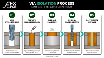
As Altium's MCPCB design guidelines document, any incomplete execution of this sequence — particularly if the insulating gel contains voids or is not fully cured before replating — creates a latent short-circuit failure mode. The board may pass initial electrical testing but fail after thermal cycling drives the void to close contact with the plated copper wall.
For single-layer MCPCBs with no interlayer routing, this step is simplified considerably — through-holes for component mounting don't require electrical isolation from the base in the same way.
Step 6: Solder Mask Application
Liquid epoxy solder mask is applied by curtain coating or screen printing, then selectively exposed and developed to open solder pads and test points while protecting all other copper areas.
The solder mask must be compatible with the thermal expansion coefficient of the metal base — a requirement that FR4-focused processes often don't account for. Aluminum's CTE is approximately 23–24 ppm/°C. A solder mask formulation not matched to this expansion rate will crack under thermal cycling — initially at pad edges, eventually compromising solder joint integrity.
Step 7: Surface Finishing and Silkscreen
Surface finishes protect exposed copper pads from oxidation and ensure reliable solderability. SFX PCB offers HASL, ENIG, OSP, and Immersion Silver across its MCPCB product line.
Finish selection guidance:
| Finish | Best For | Notes |
|---|---|---|
| ENIG | LED lighting, fine-pitch components | Flat surface; 3–6 µm Ni + min. 0.05 µm Au per IPC-4552 |
| HASL | Cost-sensitive applications | Economical; lead-free HASL available |
| OSP | Single-reflow applications | Low cost; limited shelf life and thermal excursion tolerance |
| Immersion Silver | Fine pitch; RF applications | 12-month shelf life per IPC-4553A |
ENIG is the preferred finish for LED applications. Its flat, consistent surface ensures intimate pad-to-component contact — critical when mounting heat-generating LEDs that depend on that contact for thermal transfer. The nickel barrier layer also protects against copper migration under thermal stress.
Silkscreen reference designators are applied by inkjet or screen printing after surface finishing.
Step 8: Electrical Testing and Final Profiling
Every completed MCPCB panel undergoes electrical testing before profiling. SFX PCB applies 100% electrical testing on every bare board — not sampling — using flying probe or bed-of-nails methods to verify opens, shorts, and critically, isolation between all circuits and the metal base.
This last verification point is unique to MCPCBs. Standard FR4 electrical testing checks continuity between intended nodes and absence of shorts between unintended nodes. MCPCB testing adds a third verification: isolation between all circuit nodes and the conductive metal base. Ventec's VT-4B7H specification requires Hi-Pot withstand voltage testing at >600 VDC on 100% of working panels. This is the standard that procurement specs should reference.
After testing, panels are routed, V-scored, or scored into individual boards. Conformal coating — available from SFX PCB in silicone, polyurethane, and epoxy formulations — may be applied for applications facing moisture, salt spray, chemical exposure, or temperature extremes from -50°C to 200°C.
Key Factors Affecting MCPCB Manufacturing Quality
Five variables determine whether an MCPCB performs as designed or fails under load:
- Dielectric thermal conductivity: The dielectric is the largest thermal bottleneck in the stack. Its W/mK rating must match the application's actual heat load — specifying "higher than FR4" sets a floor too low to be meaningful for any serious power application
- Metal base alloy and thickness: Alloy grade affects both thermal conductivity and CTE; mismatched CTE between metal base and circuit layers causes delamination under thermal cycling. Copper C1100 at 16.8 ppm/°C behaves very differently from aluminum 5052 at 23.8 ppm/°C, so circuit layer materials must be selected with that delta in mind
- Via isolation process control: The insulating gel fill must be fully cured and void-free before replating. Voids create latent short-circuit failure modes that surface only after thermal stress in the field — boards that pass incoming inspection can fail six months into deployment
- Surface finish compatibility: Operating temperature range and soldering method (reflow vs. wave vs. hand) both influence which finish performs reliably; not all finishes adhere equally to copper traces on a metal-core substrate
- DFM review before fabrication: Trace width, pad size, and thermal relief design decisions made at the layout stage directly shape how well the finished board dissipates heat — catching these before fab starts prevents costly respins
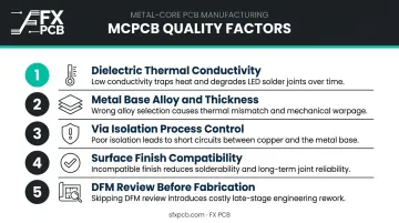
SFX PCB includes a free DFM review with every order, covering stack-up optimization, trace width, spacing, and annular ring checks before fabrication begins.
Common Misconceptions and When MCPCB May Not Be the Right Choice
Three Persistent Misconceptions
"All metal core PCBs perform the same." Aluminum 5052 conducts at 138 W/mK. Aluminum 6061 at 167 W/mK. Copper C1100 at 386 W/mK. And the dielectric layer between the circuit and that base ranges from 2.2 W/mK to 8 W/mK depending on formulation. A board labeled MCPCB is not automatically a thermal solution — the specific material stack determines performance.
"MCPCBs can replace FR4 in any design." MCPCBs are limited in layer count and routing complexity. High-signal-density digital boards, RF multilayer designs, and anything requiring more than 2–4 circuit layers with complex interconnects don't benefit from a metal core. The result is added cost and manufacturing complexity with no proportional thermal payoff.
"Standard PCB manufacturers can produce MCPCBs." Via-plugging, dielectric lamination to metal, and etchant compatibility all require dedicated process equipment and validated parameters. Manufacturers without MCPCB-specific tooling will produce unreliable boards even when they accept the order.
When MCPCB Is the Wrong Choice
Understanding these misconceptions makes the decision clearer. MCPCB is a targeted solution — not a universal upgrade. These are the scenarios where FR4 is the better call:
- Low-power applications where FR4 with thermal vias handles heat adequately
- Multilayer designs with dense signal routing that exceed MCPCB's typical 2–4 layer ceiling
- Situations where the conductive metal base introduces grounding or EMI complications not addressed in the design
- Prototype phases where MCPCB tooling cost and lead time aren't yet justified — SFX PCB's prototype lead time for aluminum MCPCBs runs 5 working days for single-sided and 14 working days for double-sided designs
Conclusion
MCPCB manufacturing is a precision sequence where the metal core — the board's strength, its heat spreader, and its primary short-circuit risk — demands purpose-built steps at every stage. Standard FR4 fabrication knowledge gets you through imaging and etching. It doesn't prepare a manufacturer for the via isolation sequence, the dielectric lamination parameters, or the isolation-to-base electrical testing that distinguishes a reliable MCPCB from one that fails in the field.
When selecting a manufacturer, these three factors carry as much weight as the board design itself:
- Verified MCPCB-specific process controls (not adapted FR4 workflows)
- Certified quality systems — ISO9001, ISO13485, and IPC-A-610 compliance
- 100% electrical testing on every bare board before shipment
SFX PCB brings over 15 years of metal core PCB manufacturing experience across aluminum, copper, and composite base materials, with copper weights from 1 oz to 10 oz. Every order includes a free DFM review, with full capabilities from bare board fabrication through conformal-coated assembly.
Frequently Asked Questions
How are 4-layer metal core PCBs made?
Multilayer MCPCBs are built by bonding additional dielectric and copper layers to each side of the metal core. Layer transitions through the metal require the oversized-hole/insulating-gel/cure/replate sequence to prevent shorts, making multilayer MCPCBs significantly more complex and costly than FR4 — which is why practical layer counts are typically limited to 2–4.
What is the outer layer of a metal core PCB?
The outermost visible layers are the solder mask (protecting copper traces) and silkscreen (reference designators), with the circuit copper layer beneath, then the thermally conductive dielectric, and the metal base at the bottom. The metal base underside is typically exposed or anodized for direct heat sink contact.
What is the 3W rule in PCB design?
The 3W rule states that spacing between two traces should be at least 3 times the trace width to reduce electromagnetic coupling and crosstalk. In MCPCB designs, it still applies — but the conductive metal base can affect signal return paths, so stackup-specific validation is required rather than relying on the rule alone.
What is the most common metal used in metal core PCBs?
Aluminum — typically 5052 or 6061 alloy — is the dominant choice, accounting for the majority of MCPCB production. Its combination of thermal conductivity (138–167 W/mK), low weight, machinability, and cost makes it practical for LED lighting, automotive, and power electronics. Copper is reserved for applications where maximum thermal performance justifies its higher cost and weight.
How is drilling in MCPCB different from standard PCB drilling?
In standard PCBs, drill bits pass through non-conductive fiberglass without creating shorts. In MCPCBs, any via penetrating the metal core must be drilled oversized, filled with insulating epoxy gel, fully cured, re-drilled to final diameter, and copper-plated — a multi-step isolation process with no FR4 equivalent and the most common source of field failures when done incorrectly.