
The challenge is that QA in PCB assembly isn't a single inspection step. It's a layered system that starts before the first component is ever placed and doesn't end until the board has been validated under real operating conditions. Engineers, product managers, and procurement teams need to understand what that system looks like — and what it costs when any layer is missing.
This article walks through each QA layer in sequence: pre-production DFM analysis, component sourcing controls, in-process inspection (SPI, AOI, X-ray), final electrical and functional testing, and the certifications that signal whether a manufacturing partner actually operates these processes or just claims to.
Key Takeaways
- DFM analysis eliminates design-sourced defects before production begins — the highest-ROI QA step available
- SPI and AOI catch solder paste and placement defects at the point of lowest rework cost
- X-ray inspection is the only non-destructive method for verifying hidden solder joints under BGA and QFN packages
- ICT and FCT validate structural integrity and real-world functional performance, in that order
- IPC-A-610, ISO 9001, and ISO 13485 certifications are verifiable signals of QA maturity — not marketing claims
Pre-Production QA: DFM Analysis and Component Sourcing
Designing for Manufacturability: The First Line of Defense
A DFM (Design for Manufacturability) review examines the complete design package — Gerber files, BOM, and pick-and-place data — before production starts. The goal is to catch problems that produce defects at scale:
- Insufficient pad sizes and tight pad geometry that create solder bridging risk
- Via-in-pad issues without proper copper fill
- Mixed-pitch BGA placements that complicate stencil design
- Component placement that blocks thermal pathways
These aren't rare edge cases. They're the kind of errors that get introduced when a designer optimizes for schematic clarity rather than assembly process constraints, and they compound quickly once production is running.
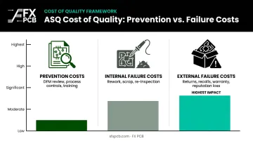
Catching a footprint error during DFM review costs the time of an engineering conversation. The ASQ Cost of Quality framework categorizes prevention costs like DFM as the cheapest quality investment possible — far below internal failure costs (rework, scrap) and external failure costs (returns, recalls). A defect that escapes to the field can trigger all three.
SFX PCB provides a free DFM analysis with every order. Engineers review Gerber files, BOM, and pick-and-place data before production is confirmed, flagging issues and recommending corrections — trace widths, stack-up, pad geometry — before any material is committed. For startups and SMEs without in-house PCB process engineers, that early review is a practical safeguard against costly surprises.
Component Sourcing as a QA Control Point
Counterfeit and substandard components are one of the most underappreciated failure modes in PCBA. They don't typically cause immediate assembly rejects — they cause latent field failures, often months after shipment, in ways that are difficult to trace.
ERAI's 2024 annual report documented 1,055 suspect counterfeit or nonconforming parts — a 25% increase over 2023. Analog ICs, programmable logic devices, and microprocessors consistently represent more than half of reported counterfeit part types. These aren't obscure components; they're the kind of parts on most complex assembly BOMs.
Best practices for component sourcing QA include:
- Authorized channels only — purchase from franchised distributors or their authorized networks, not open-market brokers, for ICs and other high-risk parts
- Certificates of conformance — require CoC documentation for every line item on high-reliability builds
- Incoming inspection — verify marking, date codes, and package condition on receipt; performance testing for critical ICs before they enter the line
- Lot traceability — maintain records linking specific component lots to specific production orders
SFX PCB maintains component traceability through its production process and conducts incoming inspection as part of its ISO 9001-certified QMS — checking component marking, dimensions, and contact area quality before parts reach the assembly floor.
In-Process Inspection: Catching Defects at Every Stage
Solder Paste Inspection (SPI)
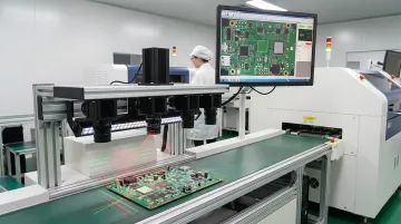
SPI is the first automated check in the SMT line. It runs immediately after stencil printing, before any component is placed, using high-precision 3D sensors to measure paste volume, height, area, and position on every pad.
This timing matters. A paste deposition problem caught here takes seconds to correct — reprint the board, verify the result, proceed. The same problem discovered after reflow requires manual rework of individual solder joints, or board scrap if the geometry won't support it.
Kester's technical documentation on defect minimization in no-clean SMT processes identifies printing-related causes behind insufficient solder, bridging, solder balling, and opens — including stencil clogging, poor print alignment, paste slump, and environmental conditions outside the recommended 70–77°F and 35–65% RH range. SPI catches these deposition failures before they become solder joint failures.
SFX PCB's SMT line incorporates SPI after the screen printing step, with the system flagging insufficient paste volume, height deviations, and misaligned deposits before component placement begins.
Automated Optical Inspection (AOI)
Post-reflow AOI uses high-resolution camera arrays to scan the assembled board and compare results against a reference or design rule set. It detects:
- Missing or wrong components
- Incorrect polarity
- Lifted leads
- Solder bridges
- Insufficient solder
- Component misalignment
AOI is fast, reliable for surface-visible defects, and generates process feedback data that helps identify systematic issues — a paste volume trend, a placement offset on a specific feeder — before they become yield problems.
The limitation is a hard one: AOI cannot see beneath components. BGA, QFN, and other hidden-pad packages are opaque to optical inspection. This is where X-ray becomes necessary.
X-Ray Inspection
Automated X-ray inspection (AXI) transmits X-ray energy through the board and produces images that reveal solder joint quality beneath packages — including voids, cold joints, head-in-pillow defects, and bridging that AOI cannot reach.
Research from Ericsson's BGA head-in-pillow study confirms X-ray as the most common non-destructive method for hidden BGA joints — but also documents its boundaries. Defect rates flagged by X-ray ranged from 0% to 38.9% across solder paste formulations, and pry-off tests confirmed far fewer actual defects than X-ray indicated. That gap is why upstream process controls matter as much as the inspection itself.
X-ray inspection is most critical for:
- Any board carrying BGA, micro-BGA, or CSP components
- Multilayer boards where internal via integrity matters
- Medical, automotive, and aerospace applications where hidden joint failures carry unacceptable risk
Final Testing Methods for PCB Assembly Validation
In-Circuit Testing (ICT)
ICT makes direct electrical contact with predefined test points on the assembled board — either through a custom bed-of-nails fixture or a flying probe system — and verifies that every component is correctly placed and within tolerance. It checks for opens, shorts, wrong component values, and missing components through direct electrical measurement.
Two configurations exist, each suited to different production scenarios:
| Method | Best For | Tradeoff |
|---|---|---|
| Bed-of-nails fixture | Medium-to-high volume runs | Upfront NRE cost; fast per-board test time |
| Flying probe | Low volume, prototypes | No fixture cost; slower throughput |
ICT validates structure and component-level accuracy. A board can pass ICT and still fail in use, which is precisely what FCT is designed to catch.
Functional Circuit Testing (FCT)
FCT is the final QA gate before shipment. The assembled board is powered up and exercised through its actual intended functions in a simulated operating environment: inputs driven, outputs measured, performance verified against the full specification.
FCT is the only test that validates the board as a system. A board can pass AOI, X-ray, and ICT (all components present, all joints structurally sound, all values in tolerance) and still fail FCT due to firmware issues, analog circuit performance, or power supply sequencing problems that no structural inspection can detect.
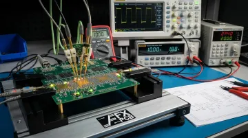
At SFX PCB, FCT fixtures are designed and built based on customer-supplied Gerber files and test specifications. The fixture uses metal probes to connect to board test points, then measures voltage, current, and signal behavior across the circuit to confirm the board meets its operational requirements.
Environmental Stress Screening
For high-reliability applications, thermal cycling, burn-in, and vibration testing expose latent defects that go undetected under normal test conditions. NASA's workmanship program documented 180 defects found on 18 mission-grade boards that had been presented as known good — an argument for stress screening even after supplier sign-off.
These tests are standard practice in:
- Aerospace and defense — MIL-STD-883 and JEDEC JESD22-A104 thermal cycling
- Medical devices — where infant mortality failures are unacceptable
- Automotive safety systems — where field reliability requirements are stringent
Industry Standards and Certifications That Signal QA Maturity
For anything beyond commodity electronics, certifications are audited commitments to documented processes — not claims. These are the standards that actually matter when vetting a manufacturing partner:
IPC-A-610 is the acceptance standard for electronic assemblies. Its three class levels define the criteria applied to every solder joint, component placement, and coating condition:
- Class 1 — General electronics where cosmetic imperfections are acceptable
- Class 2 — Dedicated-service electronics requiring extended reliability but not mission-critical
- Class 3 — High-reliability electronics (medical, aerospace, military) where continuous operation is essential and acceptance criteria are strictest
| Standard | Scope | What It Requires |
|---|---|---|
| ISO 9001 | All manufacturing operations | Documented processes, measurable quality objectives, continuous improvement |
| ISO 13485 | Medical device manufacturing | Risk management, full process traceability, regulatory-aligned documentation |
ISO 13485 carries particular weight for US-bound medical products. As of February 2026, the FDA's Quality Management System Regulation incorporates ISO 13485:2016 by reference, making it the effective US medical device QMS standard.
SFX PCB holds ISO 9001, ISO 14001, ISO 13485, IPC-A-610 Class 2/3, RoHS, REACH, and UL certifications — covering the full range required for regulated, high-reliability production across medical, industrial, and aerospace applications.
That transparency matters in practice: when evaluating any supplier, request the actual certificates rather than accepting a listed claim. Current certificates include specific scope statements and expiry dates. A credible supplier shares them without hesitation.
The Real Cost of Poor PCB Assembly Quality
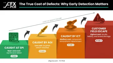
Every defect caught later in production costs more — often by an order of magnitude. Here's how the escalation pathway typically looks:
- Caught at SPI — seconds to reprint; near-zero cost
- Caught by post-reflow AOI — minutes of rework per joint
- Caught by ICT — component removal, re-solder, retest
- Caught by the end customer — RMA logistics, warranty replacement, root cause investigation, and reputational exposure
What a field escape actually looks like: A 2025 NHTSA recall (Ford recall 25V628) covered 4,632 vehicles due to battery junction box PCBs with solder mask and conformal coating failures — leading to corrosion, dendritic growth, shorts, overheating, and fire risk.
An estimated 1% defect rate across that vehicle population translated into recall logistics, regulatory scrutiny, and public visibility that no manufacturer wants.
Beyond the direct financial hit, poor PCBA quality carries non-financial costs that are harder to recover from:
- Regulatory consequences — non-compliance penalties in medical and automotive contexts
- Product liability exposure — particularly where safety-critical function is involved
- Operational disruption — a product recall consumes engineering, legal, and supply chain resources for months
- Customer trust — once a reliability failure becomes public, recovery is slow and expensive
The upfront investment in DFM review, multi-stage inspection, and certified testing costs far less than a single field escape. For boards going into medical devices, automotive systems, or industrial safety applications, that investment is the difference between a controlled process and a public recall.
Frequently Asked Questions
What is the difference between IPC-A-610 Class 2 and Class 3 in PCB assembly?
Class 2 covers dedicated-service electronics (industrial equipment, communications hardware, consumer appliances) where performance matters but uninterrupted operation isn't life-critical. Class 3 applies to medical implants, aerospace systems, and military hardware, where acceptance criteria for solder joints, component placement, and coatings are significantly stricter and continuous operation is non-negotiable.
What does AOI testing detect in PCB assembly?
AOI uses high-resolution cameras to identify surface-visible defects including missing components, wrong polarity, solder bridges, insufficient solder, and component misalignment. It cannot inspect solder joints hidden beneath BGA, QFN, or other bottom-terminated packages; those require X-ray inspection.
How does DFM analysis reduce PCB assembly defects?
DFM catches design-level problems (incorrect footprints, pad geometry that creates bridging risk, clearance violations, via-in-pad issues) before any material enters production. By eliminating the root cause of these defects at the design stage, DFM prevents entire categories of assembly failure rather than detecting them after they occur.
What are the most common causes of PCB assembly failures?
The four primary failure categories are:
- Design errors that reach production unflagged
- Substandard or counterfeit components entering the supply chain
- Solder joint defects from incorrect paste deposition or reflow profile
- Environmental stress on boards not rated for their actual operating conditions
Why is X-ray inspection important for BGA and multilayer PCBs?
X-ray reveals solder joint quality beneath BGA, QFN, and other hidden-pad packages, catching voids, cold joints, head-in-pillow failures, and bridging that are physically impossible to detect with optical methods. For multilayer boards, it also provides visibility into internal via integrity.
What certifications should I look for when choosing a PCB assembly manufacturer?
Request current certificates, not just claims, and check scope statements. At minimum, look for:
- IPC-A-610 Class 2 or 3 for assembly quality standards
- ISO 9001 for quality management systems
- ISO 13485 if the application involves regulated medical devices
- RoHS/REACH compliance for access to EU and global markets